MIP+ | Plasma Die-Level Etching
The next generation in semiconductor decapsulation and etching
Breakthrough innovation
Developed in collaboration with leading advanced packaging users.
The MIP+ machine redefines etching technology and sets a new standard in failure analysis, reliability testing and cyber security.
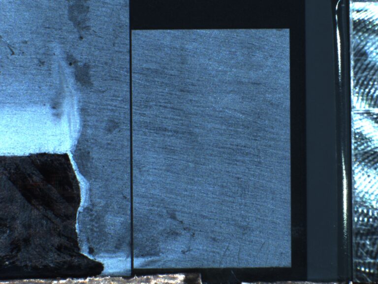
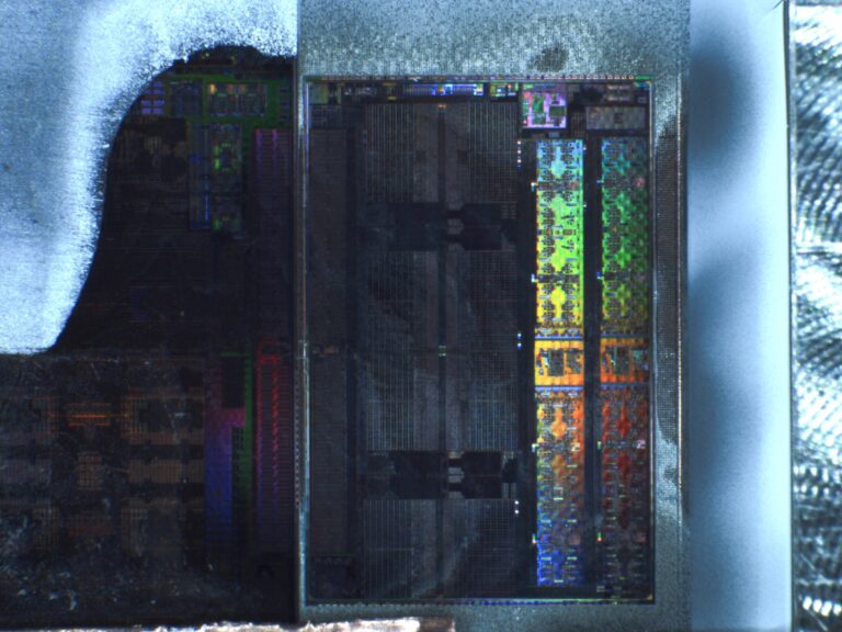
This breakthrough in plasma sample prep is achieved with new etching chemistries. These new recipes allow for die-level access, allowing JIACO Instruments to enable localized plasma etching of semiconductors, with ion-free solutions for silicon (Si), silicon dioxide (SiO₂), silicon nitride (Si₃N₄) and more advanced packages.
Unrivaled performance
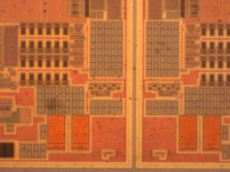
The MIP+ enables atmospheric pressure etching of inorganic and organic materials, without ion bombardment. Selectively etching advanced packaging and die materials while preserving critical underlying features, thus enabling artifact free plasma sample preparation.
Advanced semiconductor sample analysis in 3 steps
1. Get in touch
Contact us to discuss your challenge and how we can help you solve it..
2. Solution validation
We demonstrate how we can solve your challenge using your own samples, so you can see the results firsthand.
3. On site commisioning
We deliver and commission your MIP system on site, anywhere in the world.
Leader in Atmospheric Plasma Technology for Failure Analysis
Building on the renown capabilities of the MIP decapsulation system, JIACO Instruments has developed a novel solution for the etching of materials typically found in semiconductor dies, and increasingly in advanced packaging. With proven recipes and backed by a global service team, JIACO Instruments supports our customers worldwide with fast responses, and a high personal level of service.