Market developments
The Market
In recent years, semiconductor failure analysis has changed significantly. Packaging is becoming more advanced due to More-than-Moore technologies, rising gold prices, environmental legislation, stricter workplace-safety requirements and industry-wide talent shortages.
These developments have caused a major market shift. Copper (Cu), often with a palladium coating, has replaced gold as the material commonly used for wire bonds. Laboratories are also moving away from acid processes, increasing the need for a safer and more reliable decapsulation method.
Materials used as alternatives to gold in wire-bond packages are at a much greater risk of damage during acid decapsulation. This can result in inaccurate failure analysis, unreliable testing and destroyed samples before the true root cause of the problem can be identified.
These market trends are making IC decapsulation increasingly challenging—something traditional acid decapsulation can no longer keep up with.

Failure analysis
How does the MIP fit into failure analysis?
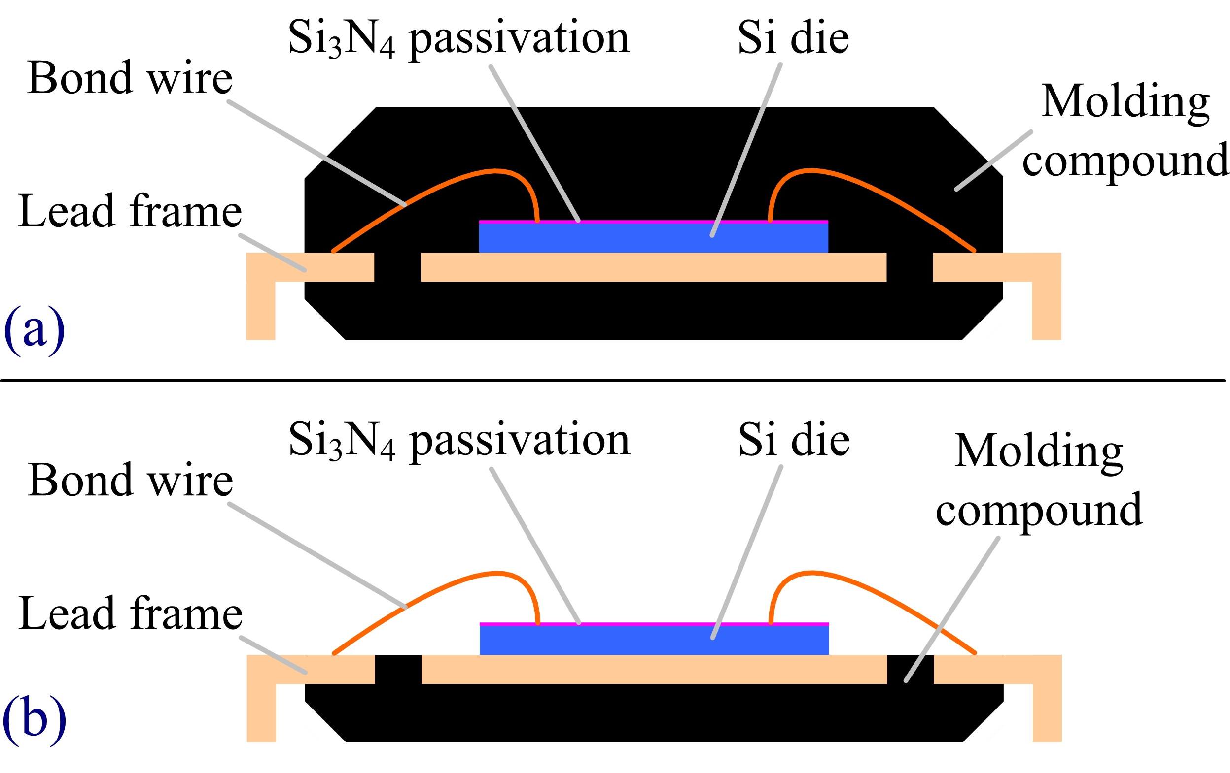
Semiconductor devices are routinely decapsulated for failure analysis and reliability testing. For plastic semiconductor packages, the epoxy molding compound must be removed selectively within a reasonable processing time.
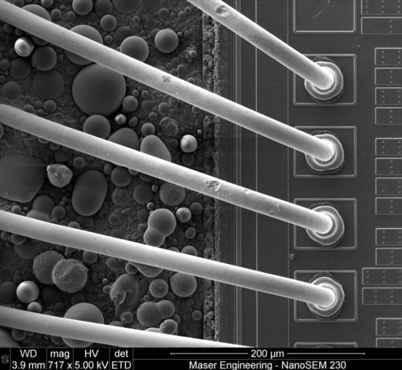
Epoxy molding compounds typically contain epoxy, silica fillers and smaller quantities of coupling agents, hardeners, releasing agents and flame retardants. During decapsulation, it is crucial that metal bond wires, aluminium bond pads, the die and the original failure site remain undamaged so that further fault-isolation methods can be performed.
These methods may include optical microscopy, scanning electron microscopy and photo-emission microscopy to locate the failure site.
If decapsulation damages any of these components, the original failure site may be altered, artefacts may be introduced and important information may be lost.
MIP decapsulation
Get it right the first time
JIACO Instruments’ patented MIP atmospheric-plasma decapsulation technology provides a crucial advantage over traditional methods. As semiconductor packaging becomes more advanced, conventional processes increasingly lack the selectivity required to protect sensitive components and original failure sites.
Our machines use oxygen and patented hydrogen-based recipes to expose and preserve components and original failure sites. MIP plasma decapsulation is highly selective and provides localised etching capabilities compared with acid decapsulation.
The process can be operated fully automatically, allowing samples to be decapsulated without continuous operator supervision.
In short, MIP enables faster and less risky operations. Protect your samples and get it right the first time.