Why are you looking for an alternative decapsulation method?
Decapsulating semiconductor devices has become increasingly challenging due to ever-changing materials, new bond wire types, and the growing complexity of package architectures. With one-off failures, highly valuable “golden samples” and stricter quality demands, the industry must evolve to meet rising customer expectations.
What does a good decapsulation process need?
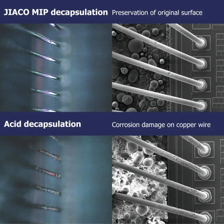
Traditional decapsulation methods such as wet chemical or acid etching often fall short, introducing artifacts, damaging devices, or even destroying original failure sites, ultimately making failure analysis results unreliable.
To meet today’s requirements, a decapsulation process must offer high selectivity, preserve both samples and failure sites, and be fully automated.
Discover MIP Decapsulation
Discover how our MIP technology delivers exactly that, contact us to learn more.
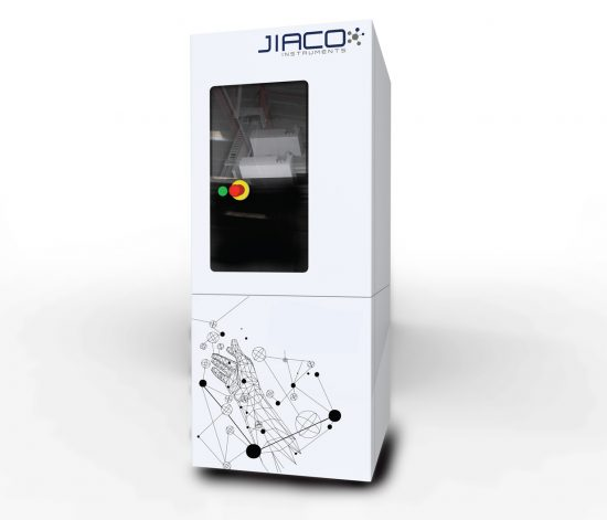
Automated atmospheric pressure MIP IC decapsulation utilizing only Oxygen and patented Hydrogen-based recipes. MIP is the global standard for tackling the semiconductor industry’s most demanding decapsulation challenges.
The Next Generation in Semiconductor Decapsulation and Etching. MIP+ extends MIP’s proven capabilities from package-level to die-level etching.
Leader in Plasma Decapsulation Technology
JIACO Instruments has over 30 papers published on MIP and plasma research, we are proud to show how the applications of our plasma decapsulation system keeps growing. Recognized by the JEDEC standard in JESD22-B120, our patented MIP technology offers non-destructive decapsulation that preserves copper and silver wire integrity. Backed by a global service team, JIACO Instruments supports our customers worldwide with fast responses, and a high personal level of service.
Rapid and accurate failure analysis is vital for maintaining brand reputation and profitability. Time, cost and talent pressures mean you only have one chance to