Methodology for Root Cause Analysis of 3D Multi-Chip Module Severely Damaged in Data Center Application
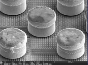
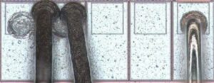
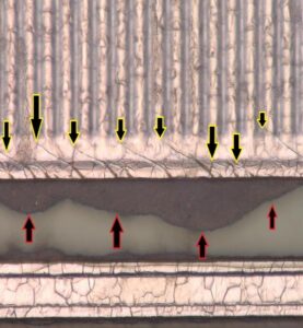
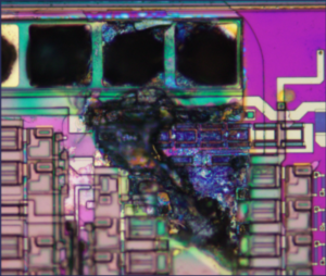
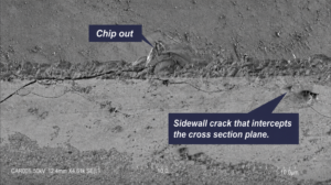
Why this paper matters At ECTC 2026, Charles Odegard from Texas Instruments will present the paper “Methodology for Root Cause Analysis of 3D Multi-Chip Module Severely Damaged in Data Center Application.” The paper focuses on the root cause analysis of a severely degraded customer-returned 3D multi-chip module used in a data center application. The