
Advanced packages, such as 2.5 and 3D architectures, enable significant improvements in performance and bandwidth, while reducing overall footprint. However, as package complexity increases, with multiple dies and components integrated into a single package, sample preparation becomes critical for ensuring subsequent failure analysis can be carried out.
2.5 and 3D packages have numerous interfaces interconnected with Cu microbumps (ubumps) and encapsulated with underfill. Often, this underfill must be removed to expose the Cu ubumps for subsequent contamination or failure analysis.
Limitations of conventional decapsulation methods
Acid decapsulation can be used for underfill removal and offers fast material removal. However, it comes with a significant risk of corroding Cu ubumps, and potential removal of contaminants. Conventional oxygen plasma based systems, typically used in fabrication environments, exhibit extremely low etching rates and require time-consuming masking for localized etching. This makes them unsuitable for the demands of failure analysis.
MIP decapsulation provides a strong alternative to acid and conventional plasma based systems to etch underfill. MIP decapsulated samples show no observable corrosion on Cu ubumps, and and the etching rate is at least 10 times the etching rate of conventional plasma based systems. Below is an indicative image from a paper published by AMD at IPFA in 2023 demonstrating the performance of MIP in etching underfill.
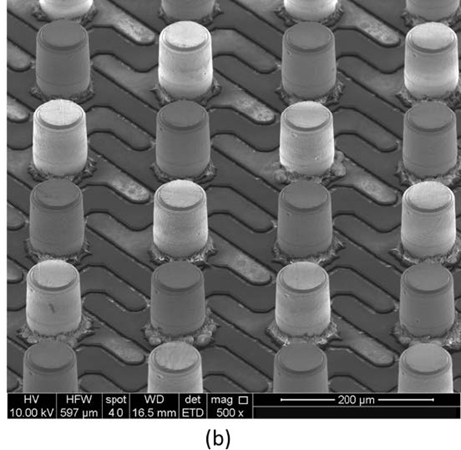
Case study: Underfill removal for Cu ubump exposure
A field return unit that failed power supply testing exhibited a localized anomaly identified with C-SAM (C-mode scanning acoustic microscopy). LIT (lock-in thermography) and LSM (laser scanning microscopy) revealed a distinct thermal hotspot and active damage in the same area.
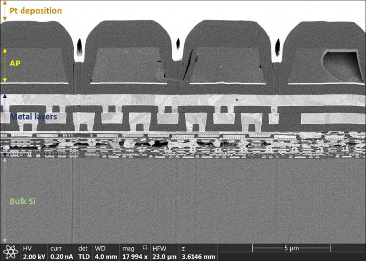
Fully exposing the defect location with mechanical grinding alone poses the risk of overgrinding and destroying the defect. To mitigate this, the sample first undergoes mechanical grinding to remove excess substrate material, followed by MIP decapsulation for precise underfill removal. SEM images of the exposed Cu ubump show no signs of damage, and the decapsulated sample continues to produce consistent results with the non-destructive tests carried out on the encapsulated sample. This confirms that MIP decapsulation preserves the failure site and does not damage the sample. Subsequent cross-sectioning reveals gross metal melt, interlayer dielectric (ILD) cracks, passivation cracks, and voids at the aluminum pad (AP), see image below.
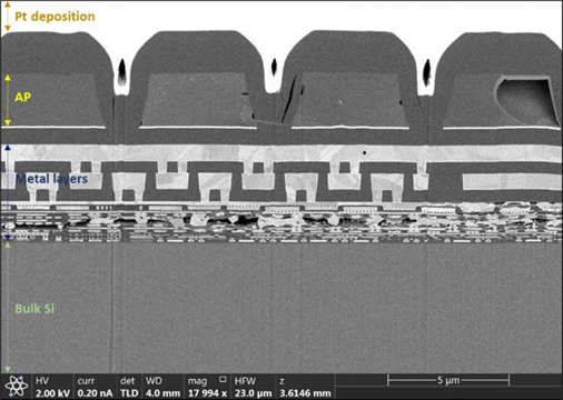
MIP decapsulation is a highly effective sample preparation technique for failure analysis of advanced packages. It preserves failure sites and does not damage Cu ubumps or die level features, enabling accurate and efficient root cause identification.
Lorem ipsum dolor sit amet, consectetur adipiscing elit. Ut elit tellus, luctus nec ullamcorper mattis, pulvinar dapibus leo.
Interested to learn more about how MIP decapsulation can be used as a sample preparation technique for advanced packages?
Learn more in this related publication:
Oxygen-Based Microwave Induced Plasma Etching for Epoxy Molding Compound Removal in Advanced Semiconductor Devices
AMD, IPFA 2023, 2.5D, 3D, Chiplet, μbump, Passivation & Die Crack, Migration & Bridging.
Need more information?
Ready to add MIP’s unique applications to your failure analysis workflow?