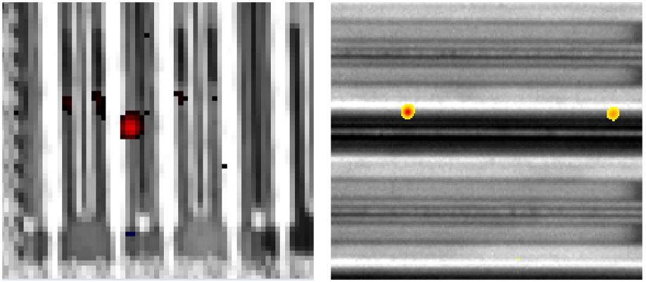
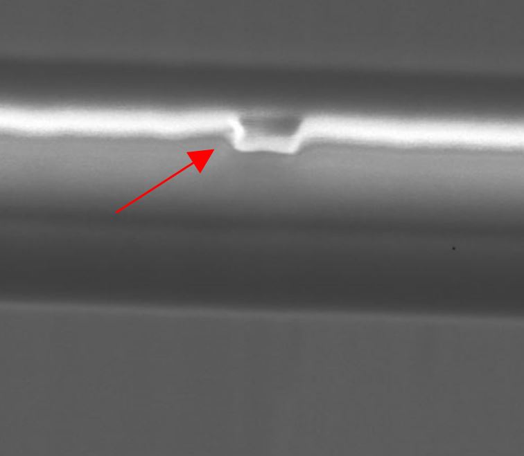
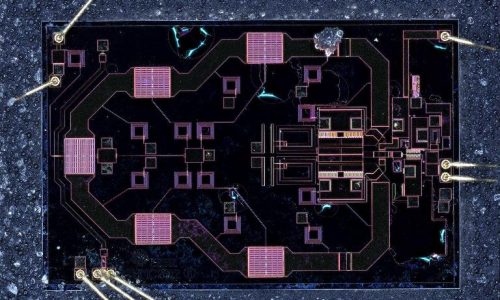
III-V power electronic devices are a growing industry as electric vehicles (EVs), power-demanding servers, and other high-power electronics become more prominent. The design of these devices can alter a failure analysis lab’s process flow
typically used on traditional silicon-based logic devices. One such obstacle is backside fault isolation (FI) through highly doped silicon wafers used in GaN-on-Si technologies. Backside fault isolation is critical for many electrical failure analyses so finding several approaches to enable this technique that fits current FA flows is desirable. Chemical and Focused Ion Beam (FIB) based approaches have been used to enable backside FI [1], [2].
This paper considers a plasma-based approach with two separate machines, a Microwave Induced Plasma spot etcher and a chamber based Reactive Ion Etch (RIE). Both utilize a Fluorine-based chemistry which is highly selective to the silicon vs the underlying GaN. The etches are used to selective remove the silicon to form a window to the underlying GaN material. Subsequent backside FI analyses are successfully followed by several other analyses.
AUTHORS
Kevin Distelhurst (GlobalFoundries. USA)
Jim Densmore (Globalfoundries. USA)
Jiaqi Tang (JIACO Instruments. Delft, The Netherlands)