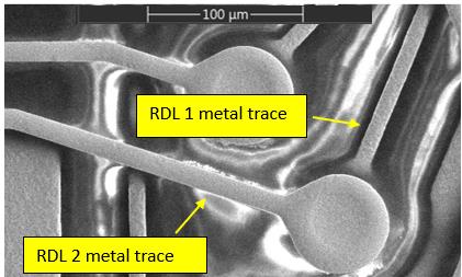
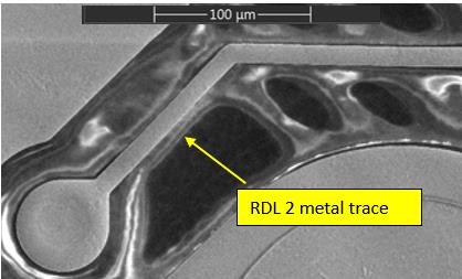
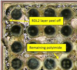
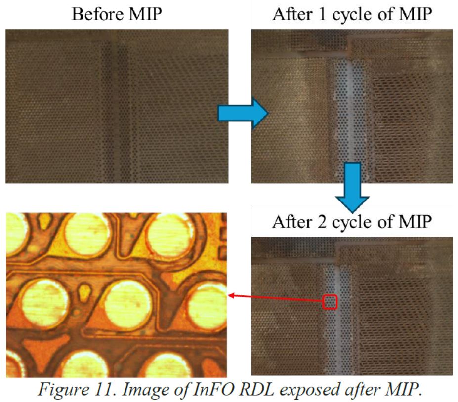
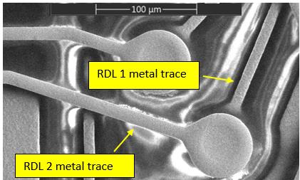
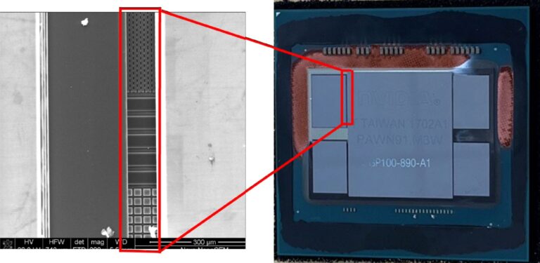
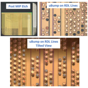
This paper describes a method to remove the polyimide layer on top of the redistribution layer (RDL) using Microwave-induced plasma (MIP) for Wafer Level Chip Scale Packaging (WLCSP). This method will help to prevent over-etching and artifact from happening on RDL metal traces. When it comes to finding a defect, especially for an open case, visual inspection will become the most important step and needs to be done thoroughly to see if there is any presence of microcrack at the RDL metal trace. Due to the smaller package size, it is difficult to detect the defect using a high-power scope due to imaging resolution.
In this paper, the inspection of RDL metal trace was done using scanning electron microscopy (SEM). The elimination of polyimide was carried out through the use of MIP by adjusting two things which is the oxygen flowrate and the number of etching cycles.
AUTHORS
Wan Nurul Asmak Binti Wan Hasnizam (Altera, Malaysia)
Siew Ming Lim (Altera, Malaysia)