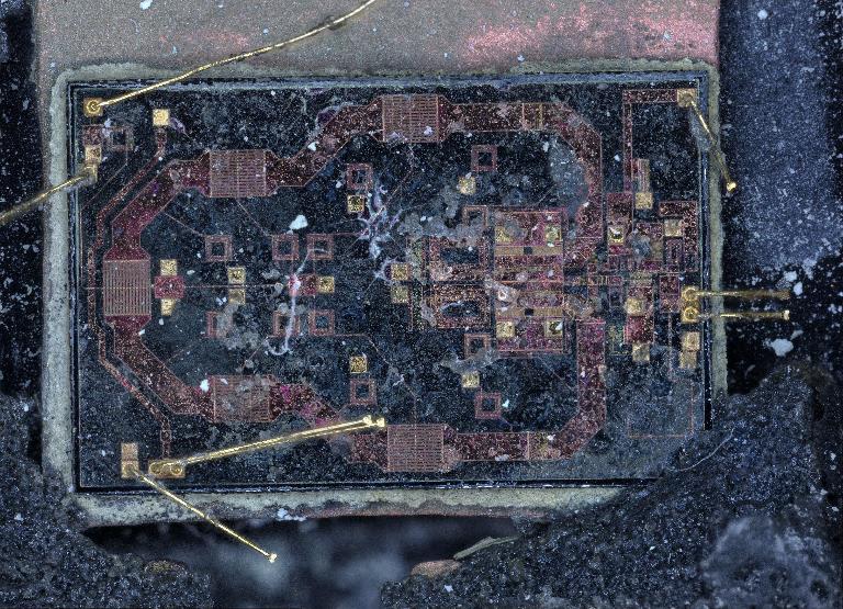
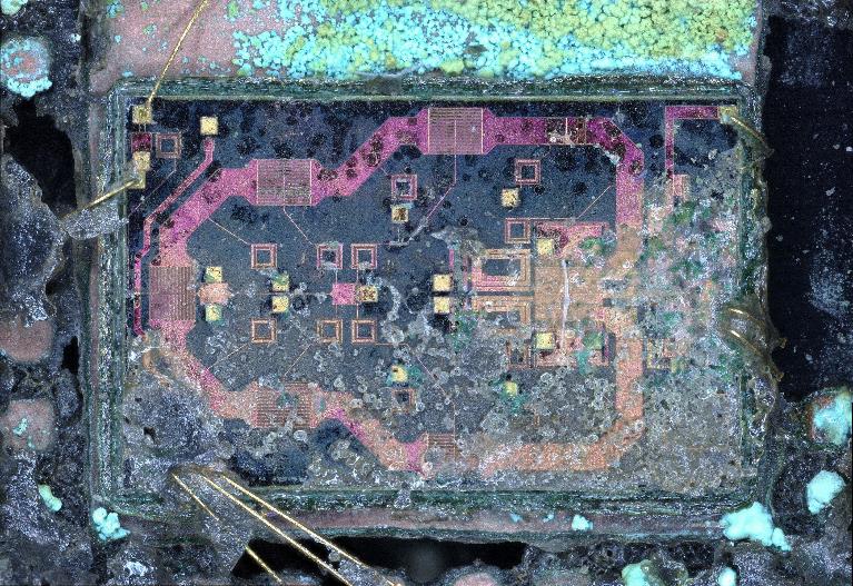
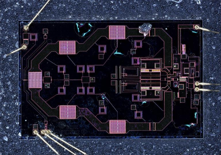
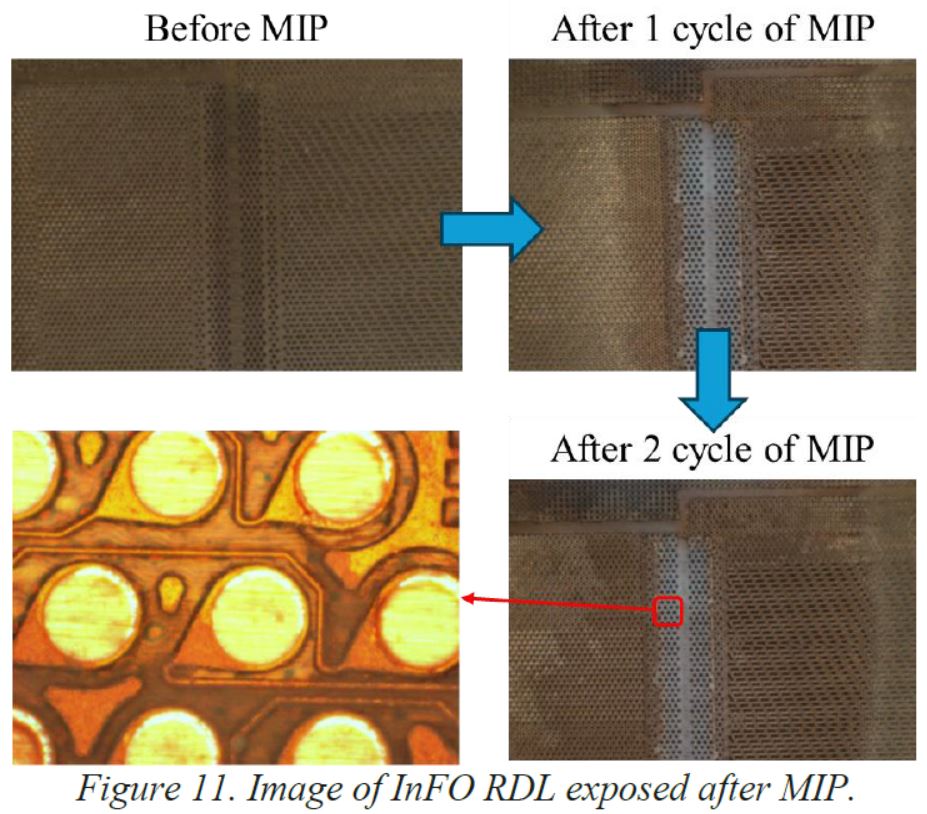
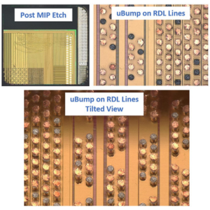
For several decades, many devices have made use of the specialized properties of Gallium Arsenide (GaAs). Unfortunately, this material presents a host of problems in the Failure Analysis field. IC package decapsulation, challenging as it is, can be further complicated by the die’s sensitivity to acid. As an alternative approach, Microwave-Induced Plasma (MIP) is a new and highly selective technology, allowing for decapsulation without the corrosion typically observed in acid decapsulation. With GaAs as a baseline being so expensive, it is vital that the failure analysis process uses up as little material as possible, while also ensuring a high rate of success from the start.
Microwave Induced Plasma systems have proven to not affect the electrical performance of the device, all while operating at atmosphere. This, in addition to the other benefits of plasma decapsulation, makes it an ideal and novel approach for these vital devices. This paper demonstrates this reliability through curve trace testing on GaAs parts before and after plasma decapsulation. In addition, a variety of samples will be compared after being exposed with traditional acid methods and an MIP system.