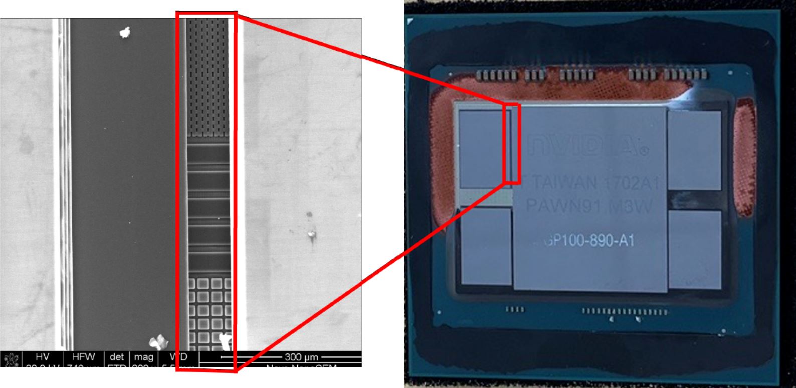
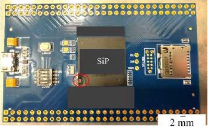
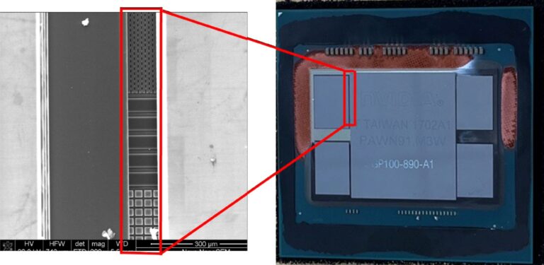
The demand for System-in-Package (SiP) devices become more prevalent in various critical and industrial applications. As a result of this growing popularity, SiP devices are becoming more attractive to attackers who are seeking to exploit vulnerabilities. Chip security is one of the cornerstones of hardware security and has received considerable attention over the past two decades. With advances in SiP-enabled advanced packaging technology, a new concept called ”security packaging of integrated circuits” has been developed to protect chips. This paper provides an in-depth analysis of SiP chip security packaging.
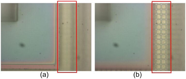
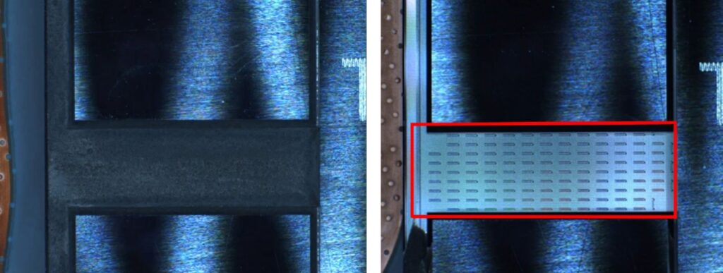
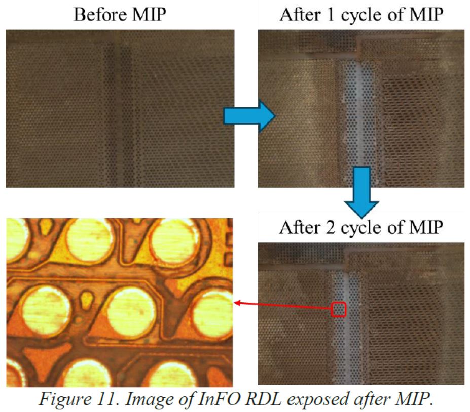
In order to accomplish this, we explore MIP sample preparation technique in an effort to ensure that vulnerable locations can be accessed. Finally, by identifying potential vulnerable interfaces, we evaluate the effectiveness of existing security measures, ensuring protection and integrity of the SiP devices. Index Terms—Advanced packaging, heterogeneous integration, system-in-package (SiP), cryptographic keys, probing, security vulnerabilities.
AUTHORS
Liton Kumar Biswas (University of Florida, Gainesville, FL, USA)
Nitin Varshney (University of Florida, Gainesville, FL, USA)
Rouhan Noor (University of Florida, Gainesville, FL, USA)
Shajib Ghosh (University of Florida, Gainesville, FL, USA)
Yashan Peng (JIACO Instruments, Delft, Netherlands)
Jiaqi Tang (JIACO Instruments, Delft, Netherlands)
Navid Asadizanjani (University of Florida, Gainesville, FL, USA)