Heterogenous integration has led to the development of advanced semiconductor packages with better
performance and smaller form factor. Such packages usually comprise of multiple dies and embedded components, which are encapsulated with epoxy molding compounds (EMCs) to improve the reliability performance and to protect the die from external impact. However, this increases the difficulty of failure analysis (FA) as the defects may manifest in the embedded components that are covered by EMCs. Suitable sample preparation techniques and workflow are required to remove EMCs to reveal the defects to determine the root cause.
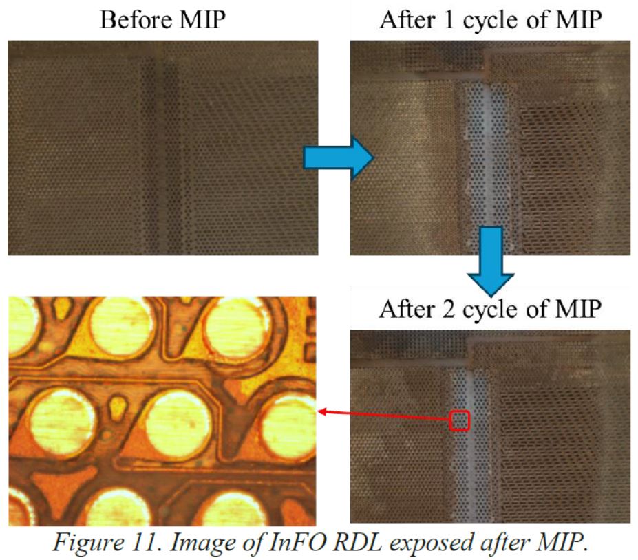
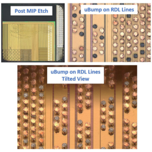
This paper explores the use of microwave induced plasma (MIP) etcher to remove EMCs. Tool parameters are varied to understand their effects on the removal rate of EMCs such as underfill.
AUTHORS
Hong Siang Tan (AMD. Singapore. Nanyang Technological University. Singapore)
Bernice Zee (AMD. Singapore)
Chee Lip Gan (Nanyang Technological University. Singapore)
Katherine Kor (Nanyang Technological University. Singapore)
Jiaqi Tang (JIACO Instruments. Delft, The Netherlands)
Mark McKinnon (JIACO Instruments. Delft, The Netherlands)