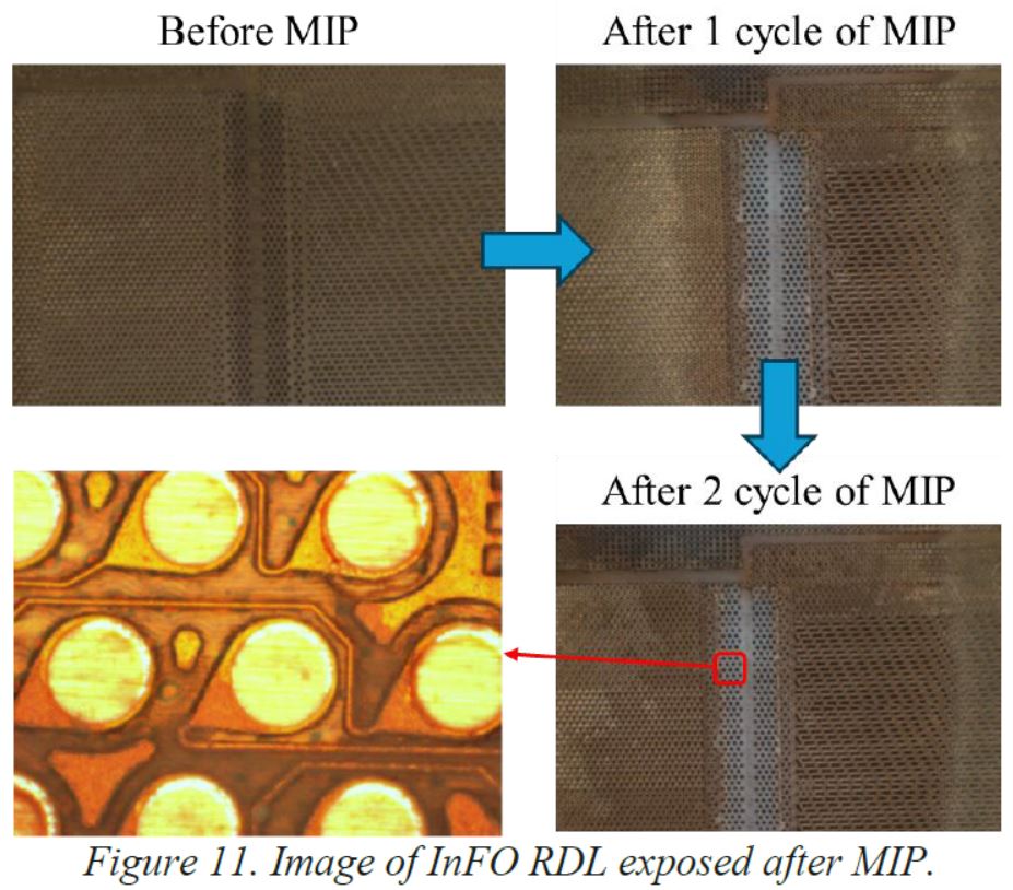
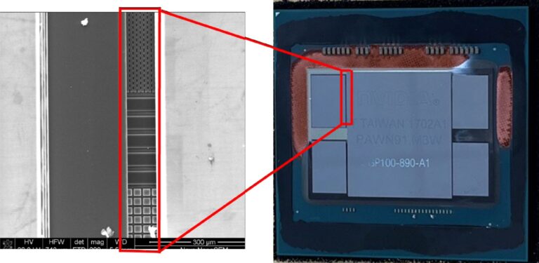
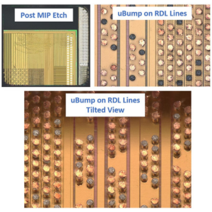
The increasing use of electronic products in IoT, SoCs, smart appliances and automotive applications, etc. raises security concerns, with hardware vulnerable to physical attacks using failure analysis (FA) tools like microprobing, fault injection, and photon emission. This paper evaluates hardware security on a system-in-package (SiP) device on a printed circuit board (PCB), with an embedded Electrically Erasable Programmable Read-Only Memory (EEPROM), focusing on physical inspection (X-ray) and sample preparation techniques such as laser decapsulation, acid decapsulation, and microwave induced plasma (MIP) etching to expose the EEPROM die or stitch pads for signal probing.
Techniques were also tested on standalone SiP and dual-in-line (DIP) packages. After laser decapsulation and MIP etching, the board functionality was retained, and the EEPROM data was successfully read. This enabled the electrical signal probing at both the chip and package level for hardware security evaluation of advanced packaging devices such as SiPs on PCBs.
AUTHORS
H.B. Kor (Nanyang Technological University, Singapore)
Q. Liu (Nanyang Technological University, Singapore)
C.L. Gan (Nanyang Technological University, Singapore)


")