IC decapsulation

The importance of the MIP machine

The Market

Over the recent years, there have been major changes in semiconductor failure analysis. Packaging getting more advanced due to More than Moore’, rocketing gold prices, environmental laws, stricter workplace safety law and talent shortages. 


These trends have caused a major market shift. Copper (Cu) with often a palladium coating has replaced gold as the material most used for wire bonds. Labs don’t want to work with acid anymore and more importantly; there is a need for a better decapsulation method.
 
The substitute materials for gold in wire bond packages are at a much greater risk of damage during acid decapsulation. Resulting in inaccurate semiconductor failure analysis, reliability testing and destroyed samples, without even getting to the root cause of the problems.  

This and other various market trends are making IC decapsulation increasingly difficult. Something that traditional acid decapsulation can’t keep up with.  

JIACO MIP machines in a row
MIP machines ready to solve customer decapsulation needs
How does the MIP fit into failure analysis?

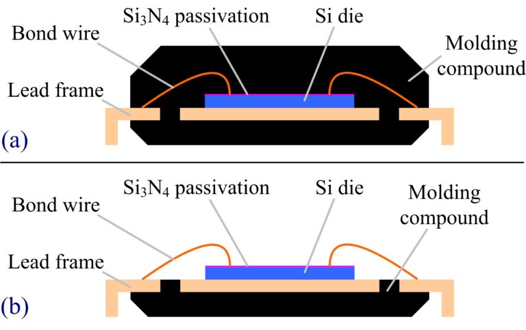
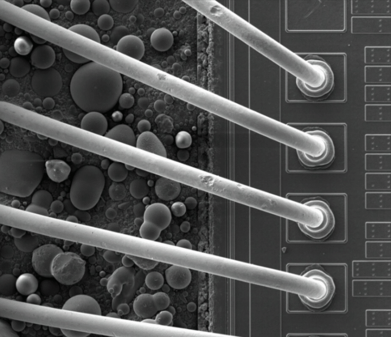
Semiconductor devices are routinely decapsulated for failure analysis and reliability test. For plastic semiconductor packages, epoxy molding compound has to be removed selectively in a reasonable processing time.

The compositions in epoxy molding compound are epoxy (10-30 %Wt), silica fillers (70-90 %Wt), and small amounts of coupling agents, hardener, releasing agents, flame retardants, etc. It is crucial that all the metal bond wires, aluminum bond pads, the die and original failure site remain undamaged during decapsulation so that further fault isolation analysis like optical microscopy, scanning electron microscopy, photo emission microscopy, etc. can be performed to locate the failure site.

If the decapsulation process causes damage to any of the above mentioned parts in the device, original failure site might be altered, artifacts might be introduced and important information might be lost.

Schematic showing how decapsulation works
Schematic representation of the semiconductor package (a) Before decapsulation; (b) After decapsulation
Wirebonds and Cu wire after being decapsulated by JIACO's MIP technology.
SEM image of PdCu wires after MIP decapsulation

Get it right the first time

JIACO Instruments patented MIP atmospheric plasma decapsulation technology has a crucial edge over traditional methods. Where these methods lack the sophistication for the increasingly more advanced packaging for semiconductors, JIACO’s plasma decapsulation machine provides the answer.
 

Our machines use only oxygen and patented hydrogen-based recipes to expose and preserve components and original failure sites. This means that our MIP plasma decapsulation technology is highly selective and has highly localised etching capabilities compared to acid decapsulation. What this also means, is that the machine is able to be operated fully automatically, allowing the machine to be left for periods of time to decapsulate samples.  


In short, the MIP enables more rapid, less risky operations. Don’t risk damaging your samples and get it right the first time.  

Leader in Plasma Decapsulation Technology

JIACO Instruments has over 30 papers published on MIP and plasma research, we are proud to show how the applications of our plasma decapsulation system keeps growing. Recognized by the JEDEC standard in JESD22-B120, our patented MIP technology offers non-destructive decapsulation that preserves copper and silver wire integrity. Backed by a global service team, JIACO Instruments supports our customers worldwide with fast responses, and a high personal level of service.

30+ peer reviewed publications

JEDEC industry standard

Excellent application support

Download our whitepaper