0 ppm failures is driving increased requirement to find the true root cause of failure in an efficient and systematic manner to support customer returns and production problems. Reliable IC decapsulation is a pre-requisite to ensure the original failure sites are preserved, requiring:
• No process-induced damage
• Preserving device electrical functionality
• Preserving original failure sites
• Preserving bond wires (Cu, Ag, PCC, Au)
• Localized decapsulation MIP (CF4-free) No damage
• Ability to handle advanced packages
• Clean removal of high Tg mold compound
Learn more about our automotive decapsulation solutions in these papers on:
The consumer & communication electronics are rapidly evolving. As the packaging and materials used to satisfy consumer demands is ever changing, reliability test & failure analysis demands are increasing due to:
– IC packages becoming smaller and increasing in complexity (SiP, 3D packaging, WLCSP, etc.)
– Shift from wire bonded to non-wire packages (WLCSP, TSV’s, 3D stacked die)
– Bond wire material changes due to increasing prices (Shift from Au to Cu to Ag)
– Newer manufacturing technologies (GaAs, SAW/BAW filters)
– Reliability requirements are rising, requiring: no process-induced damage, preservation of device electrical functionality, and the preservation of original failure sites
Learn more about our consumer & communication decapsulation solutions in these papers on:


When preparing samples for Failure Analysis, traditional decapsulation methods are no longer suitable, jeopardizing your further analysis steps. Acid decapsulation often destroys the original failure site and introduces external artifacts, making your sample analysis unreliable. CF4 based plasma decapsulation systems risk fluorine over-etch of Silicon, Silicon Nitride Passivation etc.
JIACO Instruments MIP decapsulation:
– Preserves the original failure sites on your sample, such as contamination, corrosion, and migration
– Does not introduce any external artifacts.
– Enables reliable sample analysis
– Gets it right the first time.
Learn more about our failure analysis decapsulation solutions in these papers on:
Devices used in the complex aerospace and defense industry not only need to handle long lifespans of service with complete reliability, but are also exposed to extreme conditions of temperature, pressure, and wear. Reliable and repeatable IC decapsulation is a prerequisite to ensure accurate analyses and reliability testing, requiring:
• No process-induced damage
• Preserving device electrical functionality
• Preserving original failure sites
• Preserving bond wires (Cu, Ag, PCC, Au)
• Localized decapsulation
• Ability to handle advanced packages
• Clean removal of high Tg mold compound
Learn more about our aerospace & defence decapsulation solutions in these papers on:


JIACO Instruments MIP machine allows for the sample preparation of advanced packages used in High-performance computing. Our MIP machine has been proven to be able to etch underfill materials, preserve structures in stacked-die packages, such as 2.5D and 3D and ubumps. The high selectivity enabled by the CF4-free plasma used in the MIP decapsulation allows for a reliable analysis of your sample, the first time right.
Learn more about our high-performance computing decapsulation solutions in these papers on:

Accessing and extracting critical data from IC’s under investigation is increasing in complexity due to the changing materials, smaller packages, more highly integrated designs. Reliable IC decapsulation is a prerequisite for forensic investigation, requiring:
• No process-induced damage
• Preserving device electrical functionality
• Preserving stored data in memory
• Localized decapsulation
• Ability to handle advanced packages such as SiP and 3D stacked dies
Learn more about our cyber security decapsulation solutions in these papers on:

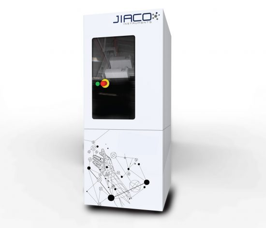
MIP | IC Decapsulation
Automated atmospheric pressure MIP IC decapsulation utilizing only Oxygen and patented Hydrogen-based recipes. MIP is the global standard for tackling the semiconductor industry’s most demanding decapsulation challenges.

MIP+ | Die Level Etching
The Next Generation in Semiconductor Decapsulation and Etching. MIP+ extends MIP’s proven capabilities from package-level to die-level etching.

Discover the new industry standard for semiconductor failure analysis