- May 19–20, 2026 | Halle, Germany | Presenting
Advancing Sample Preparation for 2.5D/3D Packages
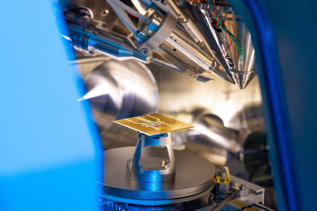
JIACO Instruments participated in the 13th CAM Workshop in Halle, Germany, bringing together specialists working in failure analysis and material diagnostics for electronic components.
During the technical programme, Jiaqi Tang presented:
“Microwave Induced Plasma Etching for 2.5D/3D Advanced Package Sample Preparation”
The presentation demonstrated how localized Microwave-Induced Plasma etching can support controlled access to regions of interest across package-, die-, and board-level failure analysis workflows.
Applications Presented at CAM Workshop 2026
01 — Flexible Access Strategies
Localized MIP etching can support top-down, bottom-up, and cross-sectional sample preparation, allowing the access strategy to be adapted to the package structure and analytical objective.
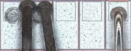
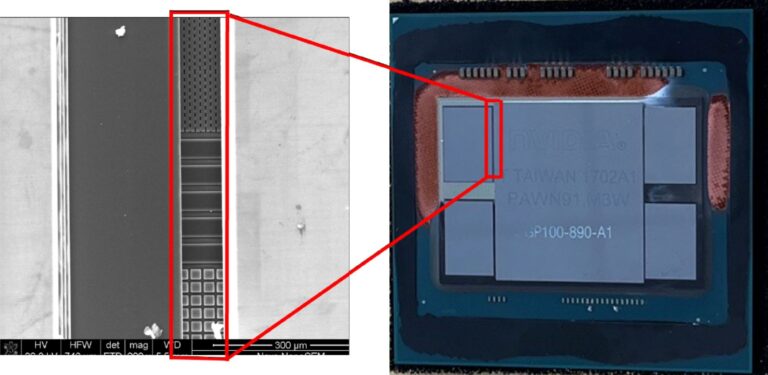
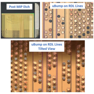
02 — Underfill Removal in CoWoS Packages
Controlled underfill removal was presented as a method for exposing µbumps and dies in CoWoS packages while supporting further inspection and failure analysis.
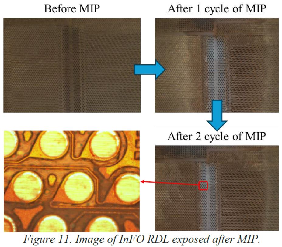
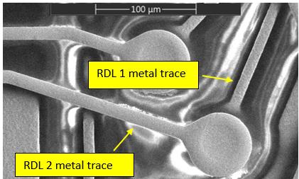
03 — Copper RDL Access in InFO Packages
Selective polyimide removal can provide access to copper redistribution layers in InFO packages while helping preserve the structures required for subsequent analysis.
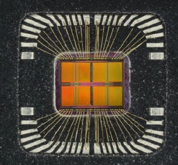
04 — Die- and Board-Level Preparation
The presentation also covered selective silicon removal, backside access for silicon and GaN-on-silicon devices, bridge-die fault isolation, and silicone sealant removal from PCBs and flex cables.
Looking Back at CAM Workshop 2026
CAM Workshop provided a focused environment for exchanging technical insights with specialists working on increasingly complex failure analysis and sample preparation challenges.
For JIACO Instruments, the event was an opportunity to demonstrate how MIP and MIP+ technologies can support controlled material removal across advanced packages, semiconductor devices, and board-level assemblies.
The applications presented illustrate how the preparation method can be adapted to the material stack, region of interest, and analytical requirements of each sample.
Let's Continue the Conversation
Thank you for visiting JIACO Instruments. Whether we met at a conference, exhibition, workshop, or technical presentation, we look forward to continuing the conversation.
Our team supports engineers, researchers, and failure analysis specialists with advanced semiconductor sample preparation, controlled material removal, and access to critical structures.