𝗜𝗣𝗙𝗔 𝟮𝟬𝟮𝟱: 𝗰𝗼𝗹𝗹𝗮𝗯𝗼𝗿𝗮𝘁𝗶𝗼𝗻 𝘄𝗶𝘁𝗵 𝗜𝗻𝗳𝗶𝗻𝗲𝗼𝗻 𝗹𝗲𝗮𝗱𝘀 𝘁𝗼 𝗲𝘅𝗰𝗶𝘁𝗶𝗻𝗴 𝗻𝗲𝘄 𝗽𝗮𝗽𝗲𝗿!
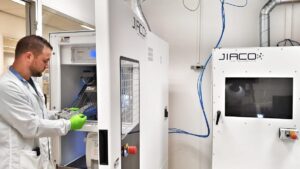
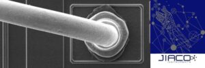
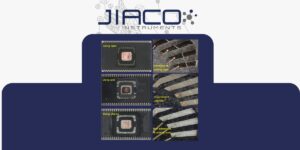
During this year’s IPFA conference we are excited to present a new paper with our customer Infineon Technologies ‘𝘙𝘦𝘷𝘰𝘭𝘶𝘵𝘪𝘰𝘯𝘪𝘻𝘪𝘯𝘨 𝘐𝘊 𝘗𝘢𝘤𝘬𝘢𝘨𝘦 𝘋𝘦𝘤𝘢𝘱𝘴𝘶𝘭𝘢𝘵𝘪𝘰𝘯 𝘸𝘪𝘵𝘩 𝘔𝘪𝘤𝘳𝘰𝘸𝘢𝘷𝘦-𝘐𝘯𝘥𝘶𝘤𝘦𝘥-𝘗𝘭𝘢𝘴𝘮𝘢 (𝘔𝘐𝘗) 𝘚𝘺𝘴𝘵𝘦𝘮’, demonstrating new solutions to the industries challenges with preserving the Nickel-plating layer on the lead finger for repackaging, preservation of Cu wires in Film Over Wire (FOW) stacked-die device decapsulation. Failure analysis involves a series of steps to identify the root cause of a failed semiconductor IC. Current methods like acid or laser etching often damage these