Abstract
Failure analysis is a collective steps and procedures used to discover the root cause of a failed semiconductor integrated circuit (IC). Amongst the many challenges faced during failure analysis, 2 challenges will be highlighted as the objectives in this study.
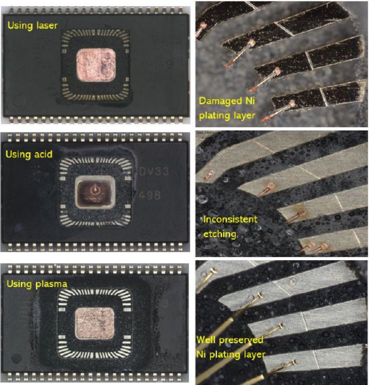
The first is to preserve the Nickel-plating layer on the lead finger during sample preparation for repackaging process. The current methods of using acid or laser tend to damage this layer which later hinders the ability for wire bonding during repackaging.
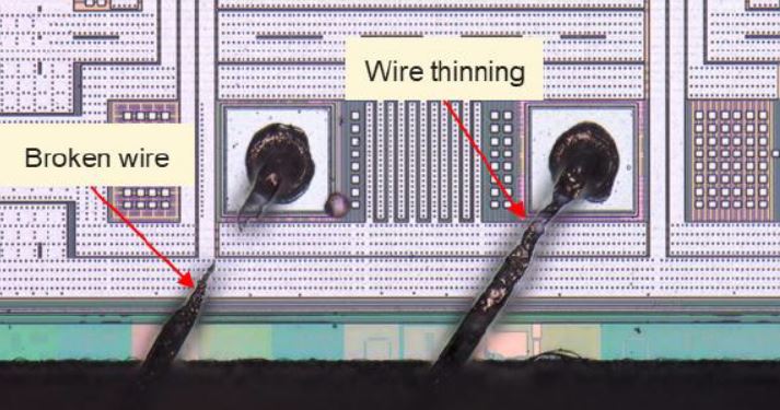
For the second, the copper wires in a stacked-die IC tend to be damaged during Film Over Wire (FOW) removal with acid etching which causes the IC to fail electrical tests and disrupts the whole failure analysis work flow.
With the methodology of using the Microwave Induced Plasma (MIP) system, the desired outcomes for both objectives could be produced with the predefined setting in the system which uses the mixture of oxygen and argon gas to form a plasma effluent that can selectively remove organic materials such as mold compound filler and polymeric materials but remains the inorganic materials such as metals.
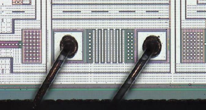
The novelty in this study is seen in the ability of the MIP to expose the lead fingers while preserving the condition of the Ni-plating layer for repackaging purpose and also seen in the ability to remove the FOW material completely while maintaining the copper wires connectivity in a stacked-die ICs.
By achieving the 2 objectives, failure analysis can be continued without any obstacles and the root cause of the failures can be effectively addressed.
Muhamad Hafiz bin Mahmud (Infineon Technologies Memory Solutions Malaysia Sdn. Bhd., Malaysia),
Muhamad Hafiz bin Rasul Kalanjiam (Infineon Technologies Memory Solutions Malaysia Sdn. Bhd., Malaysia),
Huey Lin Ong (Infineon Technologies Memory Solutions Malaysia Sdn. Bhd., Malaysia),
Jiaqi Tang (JIACO Instruments, Netherlands)