
- July 13–16, 2026 | Marina Bay Sands Convention Center, Singapore
Advancing Sample Preparation for Failure Analysis
IPFA 2026 took place from July 13 to 16, 2026, at Marina Bay Sands in Singapore. The symposium brought together the global failure analysis and reliability community for four days of technical presentations and knowledge sharing.
JIACO Instruments attended the event and engaged with engineers and researchers working on advanced failure analysis workflows, package-level analysis and semiconductor sample preparation challenges.
Together with AMD Singapore and Nanyang Technological University, JIACO Instruments contributed to the technical program with the presentation “High Throughput MIP+ Etching for Failure Analysis of SoIC Packages.”
Why IPFA Matters to JIACO Instruments
Advanced Packages Require Controlled Access
SoIC packages combine thin silicon, underfill, microbumps and stacked structures. Preparing these devices for failure analysis requires controlled material removal that exposes the region of interest while preserving critical structures and failure evidence.
Results from an Actual SoIC Package
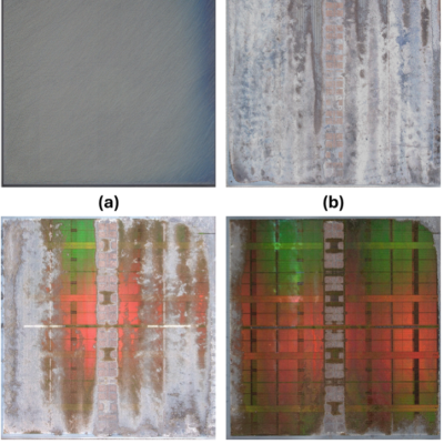
Together with AMD Singapore and Nanyang Technological University, JIACO presented an accelerated MIP and MIP+ workflow for SoIC package failure analysis. The reported process increased MIP throughput for selective underfill removal by five times compared with the baseline MIP process.
Direct Exchange with Failure Analysis Engineers
IPFA brought JIACO into direct discussion with engineers working on package-level reliability, failure analysis and sample preparation, connecting the technical presentation with practical laboratory challenges.
Looking Back at IPFA 2026
IPFA 2026 provided a valuable opportunity to connect with the international failure analysis and reliability community and discuss developments in advanced semiconductor sample preparation.
During the event, JIACO Instruments met with engineers and researchers working on package-level failure analysis and shared the application of MIP+ technology for controlled material removal.
The joint presentation by AMD Singapore, Nanyang Technological University, and JIACO Instruments demonstrated how MIP+ can support underfill removal and bulk silicon delayering for advanced SoIC packages.
To learn more about the paper or discuss a sample preparation challenge, please contact us through the website contact form or email info@jiaco-instruments.com.
Let's Continue the Conversation
Thank you for visiting JIACO Instruments. Whether we met at a conference, exhibition, workshop or technical presentation, we look forward to continuing the conversation.
Our team supports engineers, researchers and failure analysis specialists with advanced semiconductor sample preparation, controlled material removal and access to critical structures.
Read more about the paper and MIP+ applications:
High‑Throughput MIP+ Etching for Failure Analysis of SoIC Packages
By Aaron Lee, Bernice Zee, Frederick Owen Zhong, Ya-Shan Peng and Jiaqi Tang
AMD Singapore, Nanyang Technological University and JIACO Instruments