Abstract
Microwave Induced Plasma Plus (MIP+) etching provides a selective, low‑damage method for delayering advanced 2.5D and 3D SoIC packages, though throughput is limited by the small plasma effluent size. This work investigates how microwave power, gas composition, and scan speed influence material removal rate (MRR) for underfill (UF) and bulk silicon (Si). Optimized conditions—50 W power, 55 sccm O₂, and 200–225 µm/s scan speed—yield up to a fivefold improvement in UF removal.
For Si, reducing CF₄ from 90% to 80% significantly increases MRR and uniformity, with 35 W / 80% CF₄ selected as the preferred recipe. These optimized workflows improve failure analysis (FA) efficiency and sample integrity.
Aaron Lee, AMD Singapore
Bernice Zee, AMD Singapore
Frederick Owen Zhong, Nanyang Technological University
Ya-Shan Peng, JIACO Instruments
Jiaqi Tang, JIACO Instruments
FIGURES
Visual highlights from the research and analysis presented in this publication.
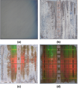
Fig. 1 – Optical microscope image of sample (a) before Si etching, (b) after bulk Si etching, (c) after multi-area etching and (d) after high-selectivity etching via MIP+.