Skip to content
  • Home
  • MIP Systems
    • MIP | Plasma Decapsulation
    • MIP+ | Plasma Die-Level Etching
  • Solutions
    • IC decapsulation
  • Applications
  • Publications
  • About us
    • About us
    • News
    • Events
  • Home
  • MIP Systems
    • MIP | Plasma Decapsulation
    • MIP+ | Plasma Die-Level Etching
  • Solutions
    • IC decapsulation
  • Applications
  • Publications
  • About us
    • About us
    • News
    • Events
GET IN TOUCH

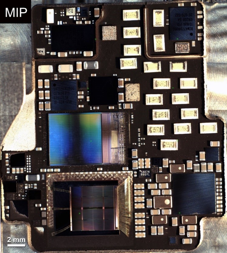
Halogen-free Microwave Induced Plasma Decapsulation of System in Package Modules

SiP undamaged after MIP decapsulation

Tech Insights, ISTFA 2017, SiP. SAW, BAW Filter, CSP, GaAs, Security Assessment.

Unique Failure Analysis Capabilities Enabled by the MIP Decapsulation Technique

EOS site exposed after MIP decap

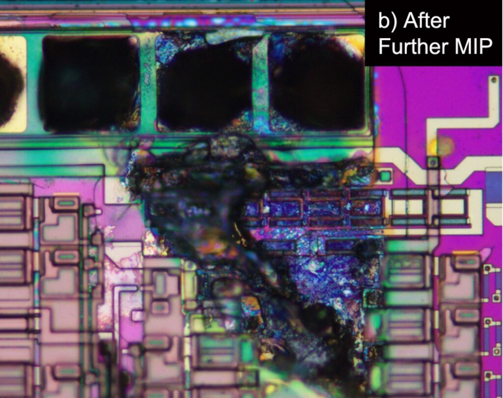
Huawei, IPFA 2017, EOS, GaAs, SiP, Contamination, Corrosion.

Delft, The Netherlands
+31 625 261 648

[email protected]

MIP

MIP+

IC Decapsulation

Applications

Publications

About us

News

Job openings

Contact

Privacy declaration