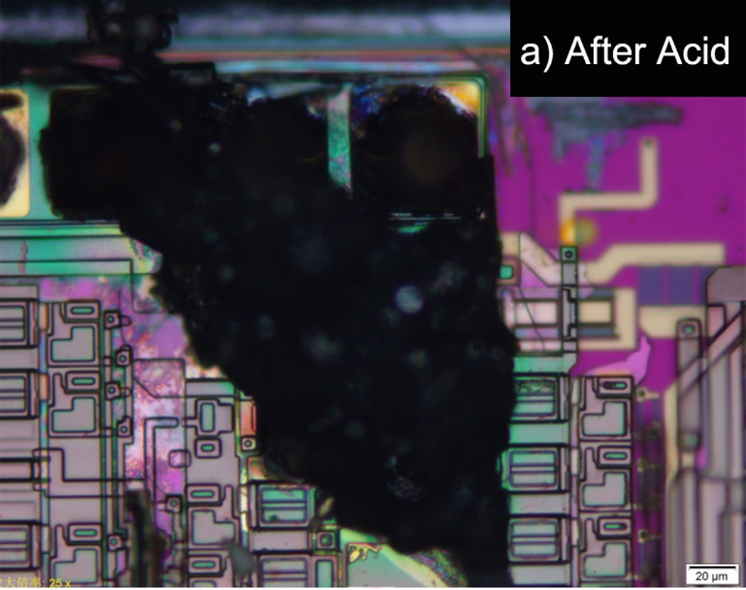
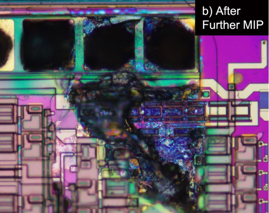
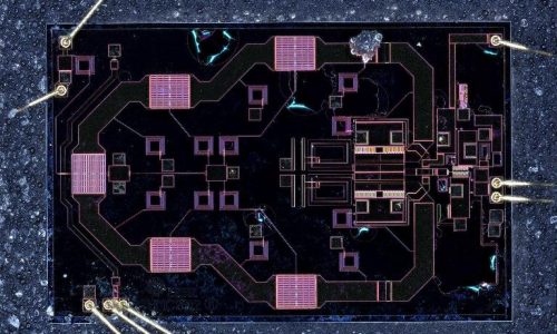
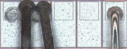
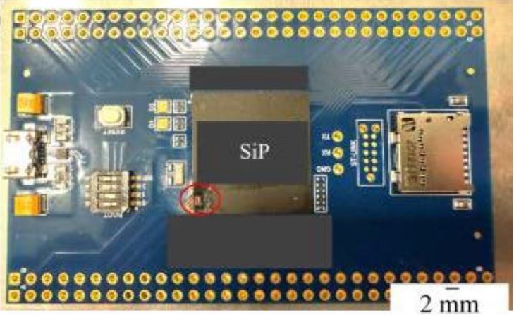
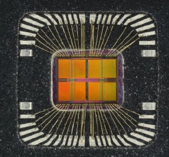
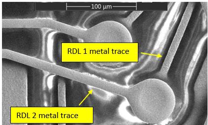
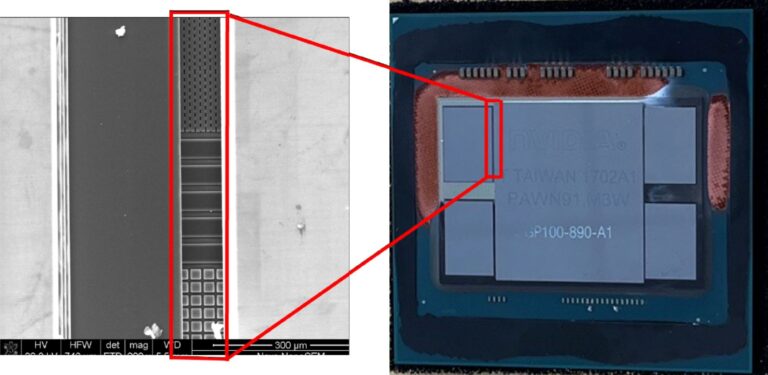
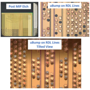
Contamination and Electrical Overstress are typical failure modes that may appear in failed devices. However, the clean exposure and excellent preservation of such failure sites is often found challenging or even impossible due to the limitations of the decapsulation techniques and tools available. The accuracy of failure analysis can be jeopardized during decapsulation due to the introduction of foreign contamination, alteration of the original failure features, and residues remaining on top of the failure sites etc.
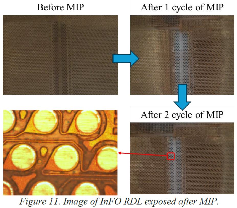
A state-of-the-art halogen-free Microwave Induced Plasma (MIP) decapsulation technique is developed and applied to challenging failure analysis cases, enabling much more accurate root cause analysis that was not possible to achieve previously.
AUTHORS
J. Tang (JIACO Instruments. Delft, The Netherlands)
B. Wang (Huawei Technologies. China)
C. Liu (Huawei Technologies. China)
J. Wang (JIACO Instruments. Delft, The Netherlands)
C.I.M Beenakker (Delft University of Technology. The Netherlands)