Removal of Highly Doped Silicon for Backside Fault Isolation with Fluorine-Based Etches
GlobalFoundries, ISTFA 2024, GaN, Migration & Bridging.
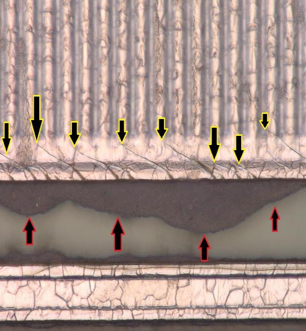
FA Challenges and Case Study Exploration of Multidie Fan-Out Wafer Level Packages
AMD, ISTFA 2024, RDL, 2.5D, 3D, Chiplet.
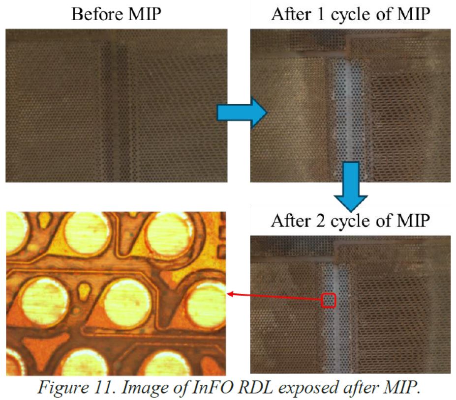
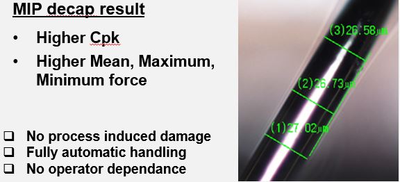
Advanced Package Sample Preparation Leveraging Precision CNC-Based Milling and Selective Microwave Induced Plasma Etching
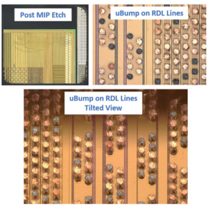
NVIDIA, ISTFA 2024, 2.5D, 3D, μbump.
Optimizations and Case Studies—Decapsulation of Hardened Epoxy SiC MOSFETs and Diodes via JIACO Microwave Induced Plasma Etching
Microchip Technologies, ISTFA 2024, High Tg Mold Compound, Passivation & Die Crack, SiC, Reliability Test.
Improving the Wire Bond Pull Test and FA for Copper Wired Components
Eurofins Maser, AEC Workshop 2024, Cu Bond Wire, AEC Q100 & Q006 Qualification, Reliability Test.