Optimizations and Case Studies—Decapsulation of Hardened Epoxy SiC MOSFETs and Diodes via JIACO Microwave Induced Plasma Etching

Microchip Technologies, ISTFA 2024, High Tg Mold Compound, Passivation & Die Crack, SiC, Reliability Test.

Abstract

One of the foremost challenges in the field of SiC MOSFET failure analysis is the effect of thermally modified mold compound on the decapsulation process. The extended total etch time that thermal modification imposes on the process of wet chemical decapsulation has created a niche for new techniques to fill.

This paper focuses on use cases for the JIACO microwave-induced plasma (MIP) etching system and how to best optimize the tool’s settings to facilitate time-efficient decapsulations. The words and data that follow aim to present what has been determined to be a successful alternative for the decapsulation of thermally modified Si and SiC power devices when wet etches prove to be ineffective.

AUTHORS

Connor J. Sorrels (Microchip Technology Inc. USA)

Kyle E. Nielsen (Microchip Technology Inc. USA)

Bret A. Walters (Microchip Technology Inc. USA)

Jiaqi Tang (JIACO Instruments. Delft, The Netherlands)

Mark W. McKinnon (JIACO Instruments. Delft, The Netherlands)
FIGURES

Visual highlights from the research and analysis presented in this publication.

1
Delamination

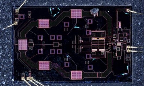
Fig. 1 — Optical inspection of the same failing SiC device. The die’s gate pad was observed to be heavily delaminated from mechanical stress (indicated by red arrows)

2
EOS on device

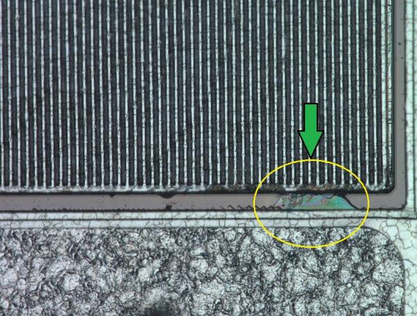
Fig. 2 — Optical inspection of the same failing SiC die. EIPD was noted between the gate pad and the nearby gate fingers (labelled by green arrow, yellow circle)

3
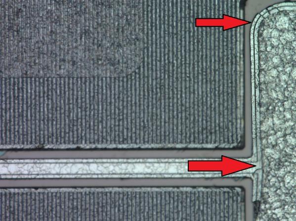
Passivation crack SiC High Tg Mold compound after MIP decap

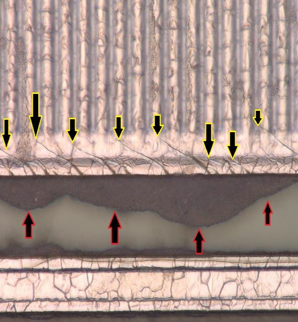
Fig. 3 — High magnification image of the failing SiC die surface following JIACO decapsulation, revealing mechanically induced passivation cracking (yellow arrows) and molten, polymerized plastic stuck to the surface of the die (red arrows)

Download this paper

Explore more publications: