
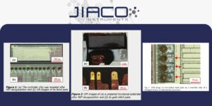
MIP: Die extraction from damaged device for package-level repair and data recovery!
At IPFA 2023, Nanyang Technological University presented “Hardware Security Assessment through Repair of Damaged Device,” demonstrating how dies from a damaged SD card, when decapsulated using JIACO Instruments’ MIP process, could be transplanted into a new package, restoring functionality and preserving the original data. The study compared acid vs. Laser + MIP decapsulation: Key takeaways: This application

MIP: Supporting Medical Devices!
Over 50% of medical devices contain electronic components, the working of these components are vital in patient care, diagnosis, and treatment. The integration of semiconductors in medical devices has revolutionized healthcare, leading to more advanced and reliable medical technologies. The quality and reliability of these semiconductors are of utmost importance, especially when it comes to

𝗛𝗼𝘄 𝘁𝗼 𝗶𝗺𝗽𝗿𝗼𝘃𝗲 𝘆𝗼𝘂𝗿 𝗳𝗮𝗶𝗹𝘂𝗿𝗲 𝗮𝗻𝗮𝗹𝘆𝘀𝗶𝘀 𝗮𝗻𝗱 𝘀𝗮𝘃𝗲 𝗰𝗼𝘀𝘁𝘀?
Our Microwave-Induced Plasma (MIP) machines don’t require specialized lab facilities, making them more cost-effective than acid decapsulation. Discover all the benefits of MIP technology by downloading our whitepaper by filling out the form below.

Another great IPFA in Penang!
From the 5th – 8th of August, our colleagues Yashan Peng and Mark McKinnon were present at 2025’s edition of IPFA in Penang, Malaysia! Yashan Peng was honored to present in the Sample Preparation for Fault Isolation User Group meeting, providing insight into how our MIP & MIP+ systems can be used for advanced package sample preparation. In her presentation

Professor Kees Beenakkers plenary talk at ICEPT 2025
On August 6th in Shangai, China, Kees Beenakker had the honour of holding a plenary talk at ICEPT 2025. In his plenary talk Prof. Beenakker looked back at over 40 years of semiconductor packaging, covering his experience in the industry from joining Philips in 1974, to co-founding JIACO Instruments, together with Jiaqi Tang, in 2014, leading to the development
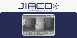
𝗠𝗜𝗣: 𝗘𝘁𝗰𝗵𝗶𝗻𝗴 𝘂𝗻𝗱𝗲𝗿𝗳𝗶𝗹𝗹 𝗺𝗮𝘁𝗲𝗿𝗶𝗮𝗹 𝘀𝘂𝗰𝗰𝗲𝘀𝘀𝗳𝘂𝗹𝗹𝘆!
Removing underfill in your devices, whether they are 2.5D/3D advanced packages, flipchips etc, enables further analysis on your samples, but can be quite challenging using traditional chemical processes.As demonstrated in many of our recent papers, our MIP & MIP+ systems can etch UnderFill (UF) material in various locations on the package to expose & preserve