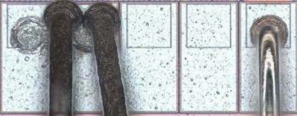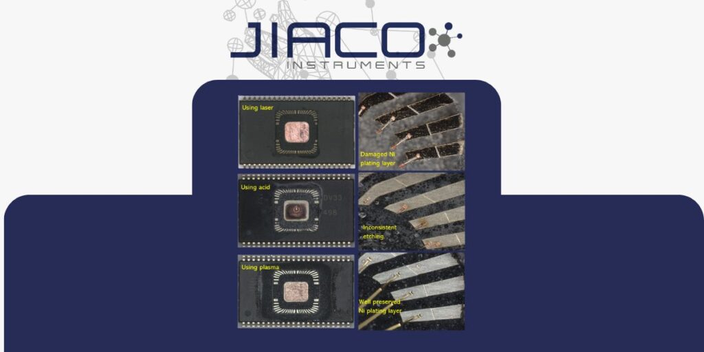
During this year’s IPFA conference we are excited to present a new paper with our customer Infineon Technologies ‘𝘙𝘦𝘷𝘰𝘭𝘶𝘵𝘪𝘰𝘯𝘪𝘻𝘪𝘯𝘨 𝘐𝘊 𝘗𝘢𝘤𝘬𝘢𝘨𝘦 𝘋𝘦𝘤𝘢𝘱𝘴𝘶𝘭𝘢𝘵𝘪𝘰𝘯 𝘸𝘪𝘵𝘩 𝘔𝘪𝘤𝘳𝘰𝘸𝘢𝘷𝘦-𝘐𝘯𝘥𝘶𝘤𝘦𝘥-𝘗𝘭𝘢𝘴𝘮𝘢 (𝘔𝘐𝘗) 𝘚𝘺𝘴𝘵𝘦𝘮’, demonstrating new solutions to the industries challenges with preserving the Nickel-plating layer on the lead finger for repackaging, preservation of Cu wires in Film Over Wire (FOW) stacked-die device decapsulation.
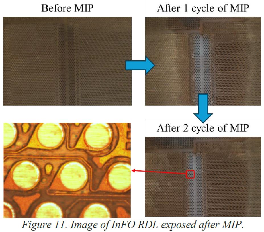
Failure analysis involves a series of steps to identify the root cause of a failed semiconductor IC. Current methods like acid or laser etching often damage these critical components. Using a Microwave Induced Plasma (MIP) system with oxygen-argon gas, this study demonstrates selective removal of organic materials while preserving metal layers. The MIP method enables continued failure analysis by maintaining sample integrity for repackaging and electrical testing.
This paper highlights some of the latest & ever growing applications & solutions enabled by the JIACO Instruments MIP decapsulation system. See the list of published papers here.