The rapid development of advanced packaging technologies for high-performance computing (HPC) applications poses
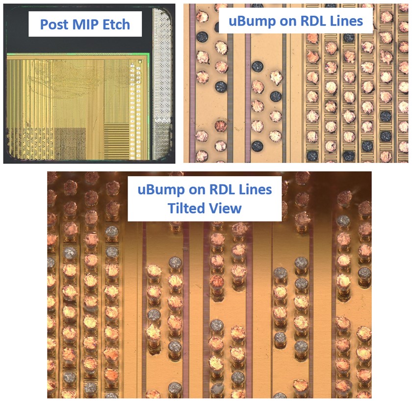
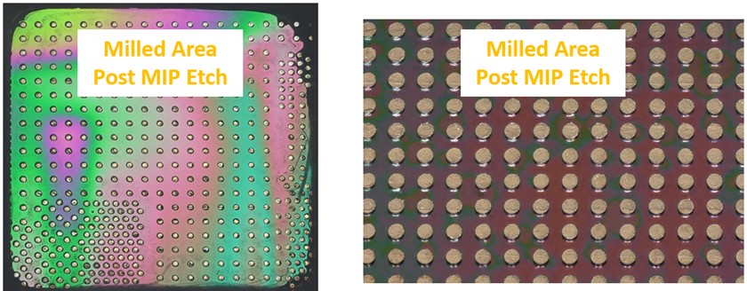
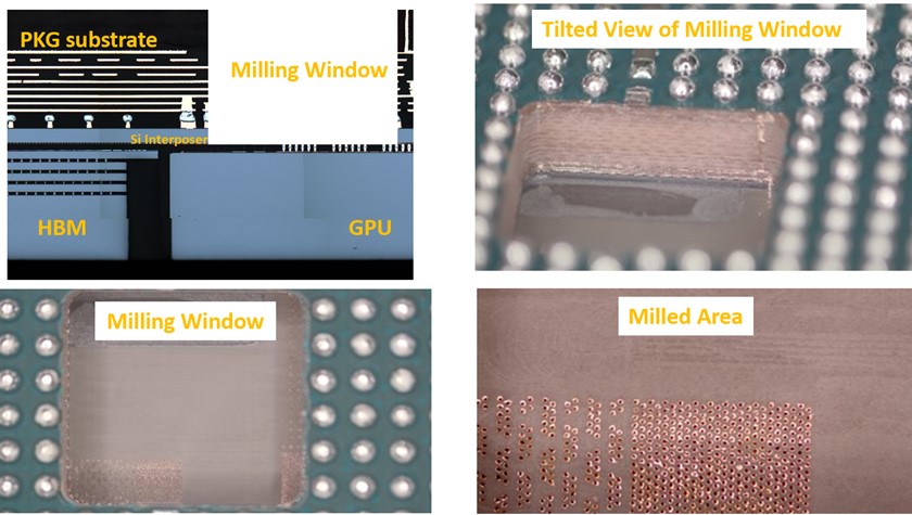
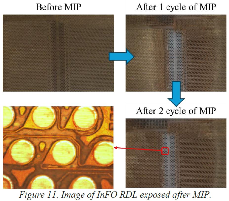
significant challenges for sample preparation methodologies. Conventional techniques are often insufficient to cope with the complex architectures and heterogeneous materials of modern packages, such as COWOS (Chip-on-Wafer-on-Substrate) and 3D structures. In this paper, we present a novel approach for sample preparation that leverages precision CNC (Computer Numerical Control) milling and selective MIP plasma etch.
These methods enable precise and selective removal of unwanted material, while preserving the integrity of the target region of interest. We demonstrate the effectiveness of our approach on various advanced packages and show how it facilitates the failure analysis tasks for HPC chips.
AUTHORS
Joseph Sanchez (NVIDIA. USA)
Chuan Zhang (NVIDIA. USA)
John Aguada (NVIDIA. USA)
Jiaqi Tang (JIACO Instruments. Delft, The Netherlands)
Chris Richardson (Allied High Tech Products Inc. USA)