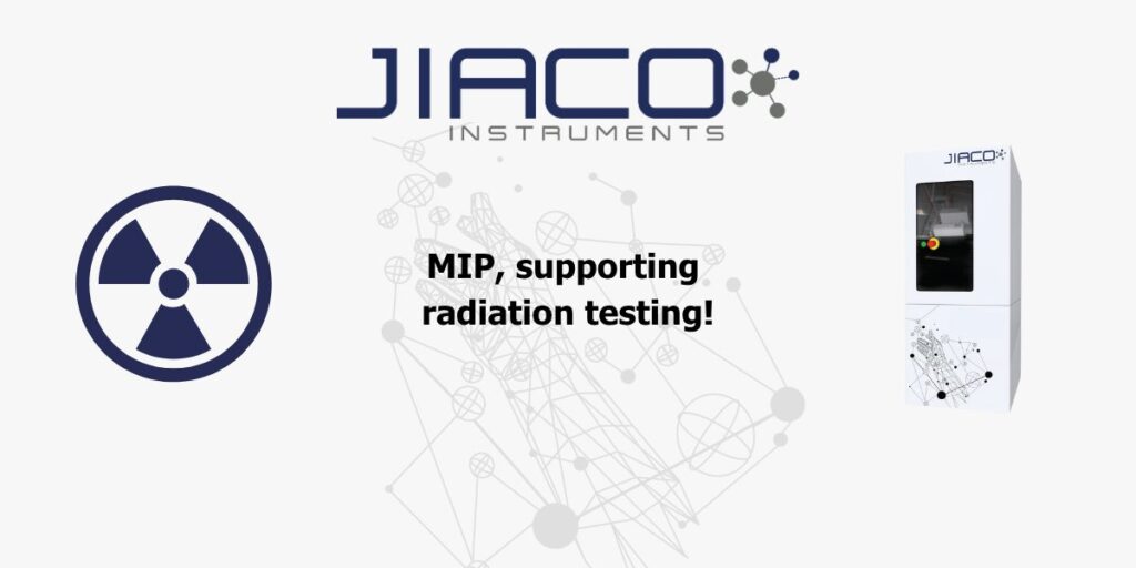
Radiation testing of semiconductors is crucial for devices used in environments with high radiation exposure, such as space or nuclear facilities. Understanding how radiation impacts your product is essential for reliability and performance.
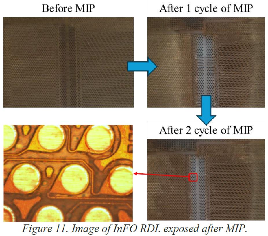
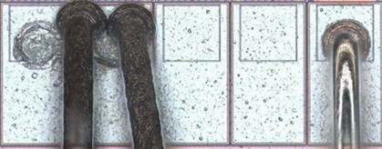
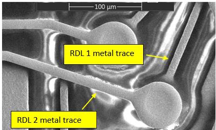
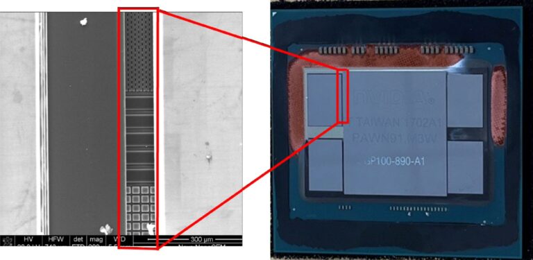
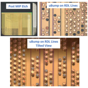
Decapsulation is necessary in radiation effects studies for semiconductors to expose the active die and allow for detailed testing & analysis of the radiation’s effects to the device. This is crucial for understanding how radiation alters the semiconductor’s electrical properties and to validate simulation models
The real challenge?
Exposing the die without introducing any damage from the decapsulation process itself.
Our MIP atmospheric plasma system enables damage-free decapsulation with high selectivity, ensuring your devices are decapsulated 1st time right so you can accurately simulate the radiation damage devices may see when in space.
𝘞𝘢𝘯𝘵 𝘵𝘰 𝘭𝘦𝘢𝘳𝘯 𝘮𝘰𝘳𝘦 𝘢𝘣𝘰𝘶𝘵 𝘰𝘶𝘳 𝘴𝘰𝘭𝘶𝘵𝘪𝘰𝘯𝘴 𝘧𝘰𝘳 𝘧𝘢𝘪𝘭𝘶𝘳𝘦 𝘢𝘯𝘢𝘭𝘺𝘴𝘪𝘴 𝘢𝘯𝘥 𝘴𝘢𝘮𝘱𝘭𝘦 𝘱𝘳𝘦𝘱𝘢𝘳𝘢𝘵𝘪𝘰𝘯?
[email protected]