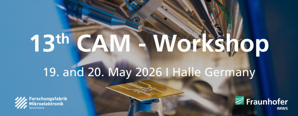
- May 19–20, 2026 | Halle, Germany
JIACO Instruments presented at the 13th CAM Workshop in Halle, Germany, a workshop focused on failure analysis and material diagnostics of electronic components.
During the workshop, Jiaqi Tang gave a technical presentation titled “Microwave Induced Plasma Etching for 2.5D/3D Advanced Package Sample Preparation”.
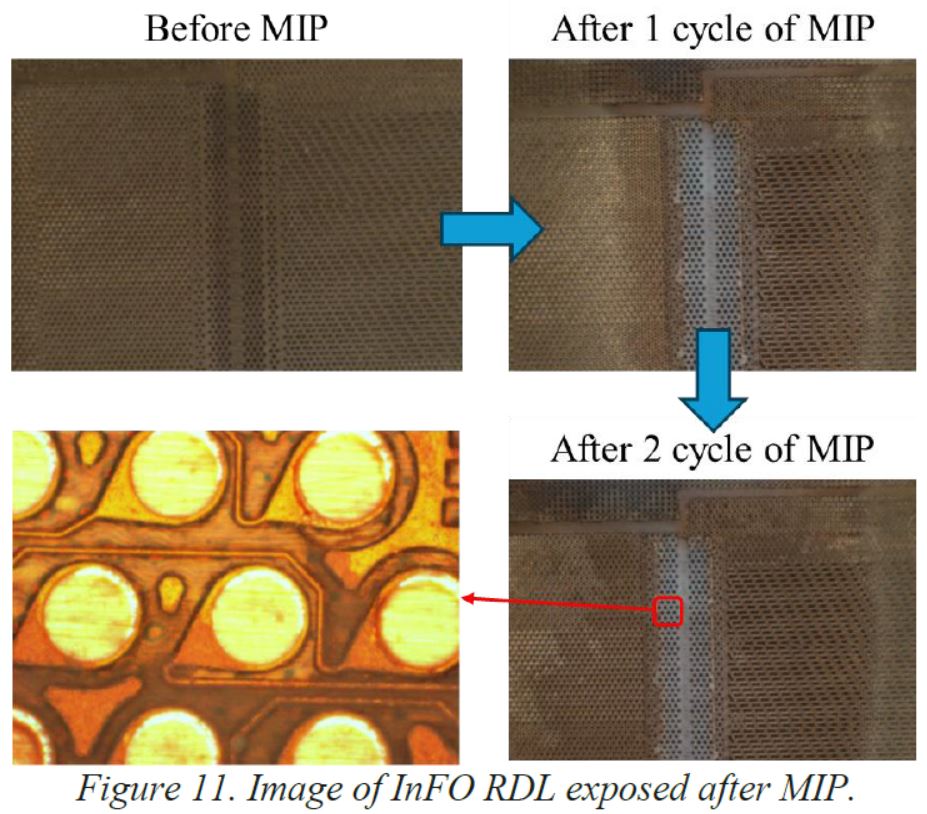
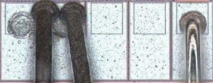
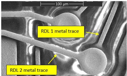
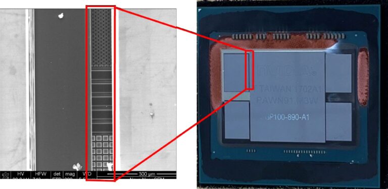
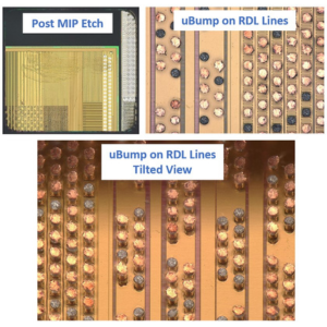
The presentation discussed the application of Microwave Induced Plasma (MIP) in sample preparation workflows, where localized MIP etching can be applied through top-down, bottom-up and cross-sectional approaches. Package-level case studies included underfill removal to expose μbumps and dies in CoWoS packages, and polyimide removal to expose copper RDL in InFO packages.
The presentation also covered recent MIP+ developments for die-level and board-level sample preparation, including selective Si removal for backside access to Si and GaN-on-Si dies, bridge die fault isolation and silicone sealant removal to access components on PCB boards and flex cables.
This presentation highlights how MIP technology can support precise sample preparation for advanced packages and complex failure analysis workflows.
Questions about the presentation or curious how MIP could support your sample preparation workflow? Contact JIACO Instruments to discuss the application, or explore more publications and technical updates below.