Abstract
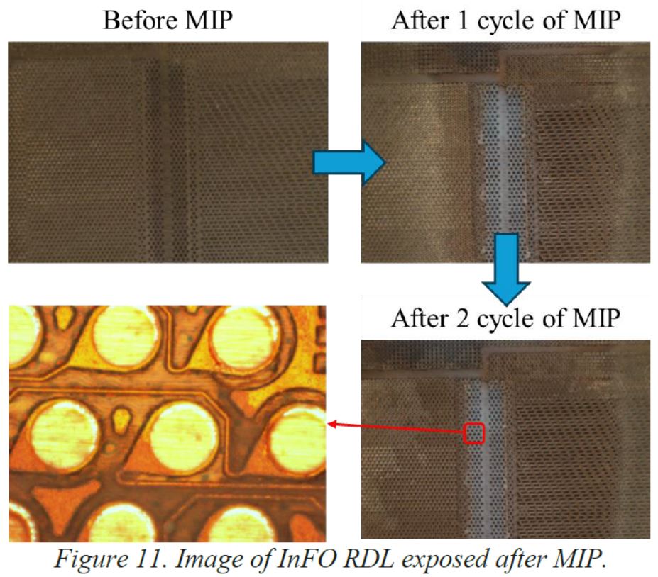
The current study demonstrates a dual-mode MIP dry etching process providing a highly selective and damage-free materials deprocessing solution for advanced semiconductor packages. By utilizing an O2 + Ar chemistry to volatilize complex organics and an Ar + O2 + CF4 mixture for the chemically driven etching of bulk silicon, the process successfully preserves delicate underlying structures such as Cu pads and SiO2 dielectrics. This methodology overcomes mechanical stress and unintended damage occurring with conventional RIE and offers a reliable sample preparation pathway critical for the advanced packaging and Si device failure analysis.
Sungmin Han, Intel Corporation
Peng Li, Intel Corporation
Jiaqi Tang, JIACO Instruments
Mark McKinnon, JIACO Instruments
FIGURES
Visual highlights from the research and analysis presented in this publication.
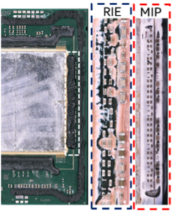
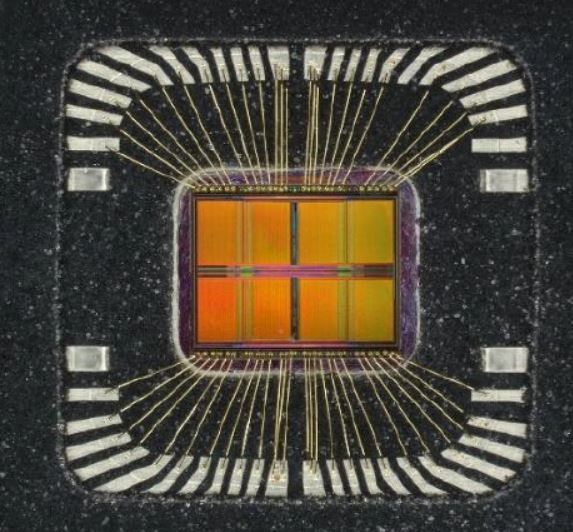
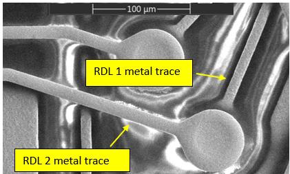
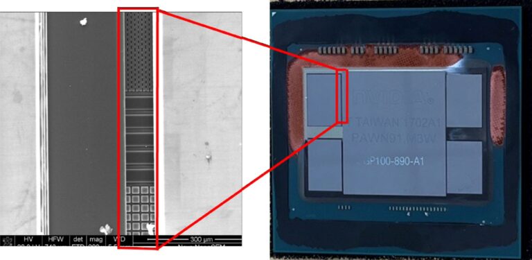
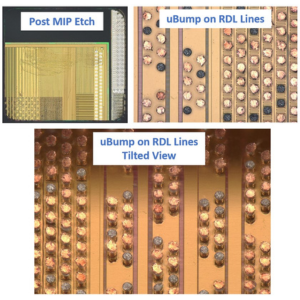
Fig. 1 – MIP selective etching on sealant encapsulant shows no damage on embedded DSC surface, comparing to RIE etching with significant damage on DSC and substrate.