Preserving the electrical functionality of devices is critical for many failure analysis workflows. When wire damage or rebonding failures cause a breakdown of the electrical functionality of devices, the analysis is often halted.
Two challenging sample preparation cases highlight how MIP decapsulation enables workflows that often fail with conventional acid or laser based techniques:
- Preserving the Nickel (Ni) plating layer on lead fingers during sample preparation for repackaging
- Film Over Wire (FOW) removal in System in Package (SiP) sample preparation.
Preserving Ni-plating on the lead frame during the repackaging process
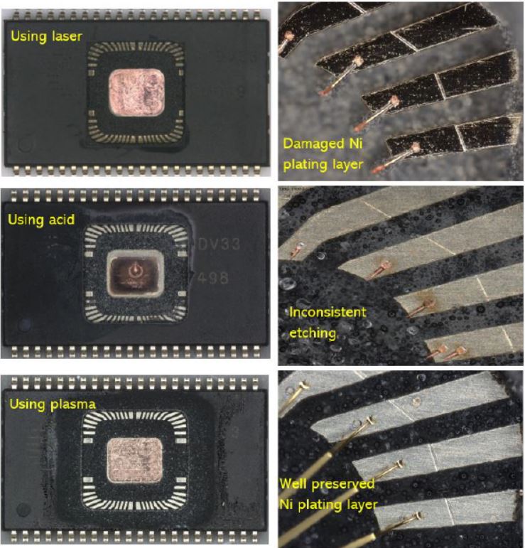
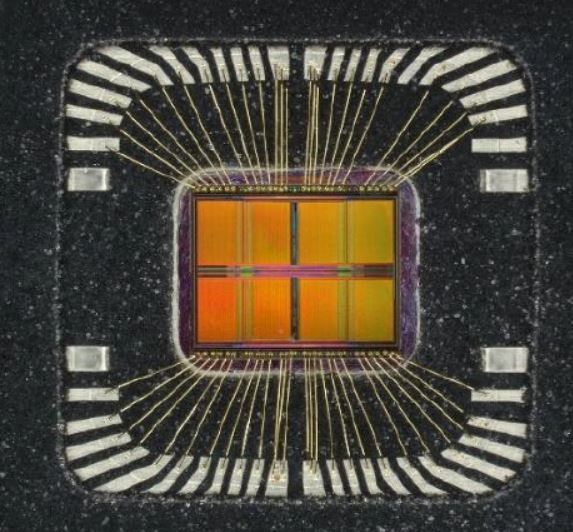
During repackaging, the die of interest is transferred from its original package into an open top package. This process involves milling an opening, removing the original die, and cleaning residual mold compound from the lead fingers before a new die can be wire bonded into place. The lead finger contains a plating material, frequently Au, Ag, or Ni, to protect against corrosion. Preserving the plating material is essential for achieving high bonding yield and mechanical reliability.
Laser decapsulation will burn and damage the Ni-plating, while acid decapsulation suffers from nonuniform removal of the mold compound, causing inconsistent Ni-plating surface exposure. Ni-plating that has been exposed to acid longer tends to oxidize faster and negatively affects subsequent wire rebonding.
In contrast, MIP decapsulation preserves the Ni-plating on the lead frames, and the subsequent wire rebonding process is successful. This allows for further failure analysis to be carried out on the repackaged Ni-plated open top device.
Removing FOW in SiP devices
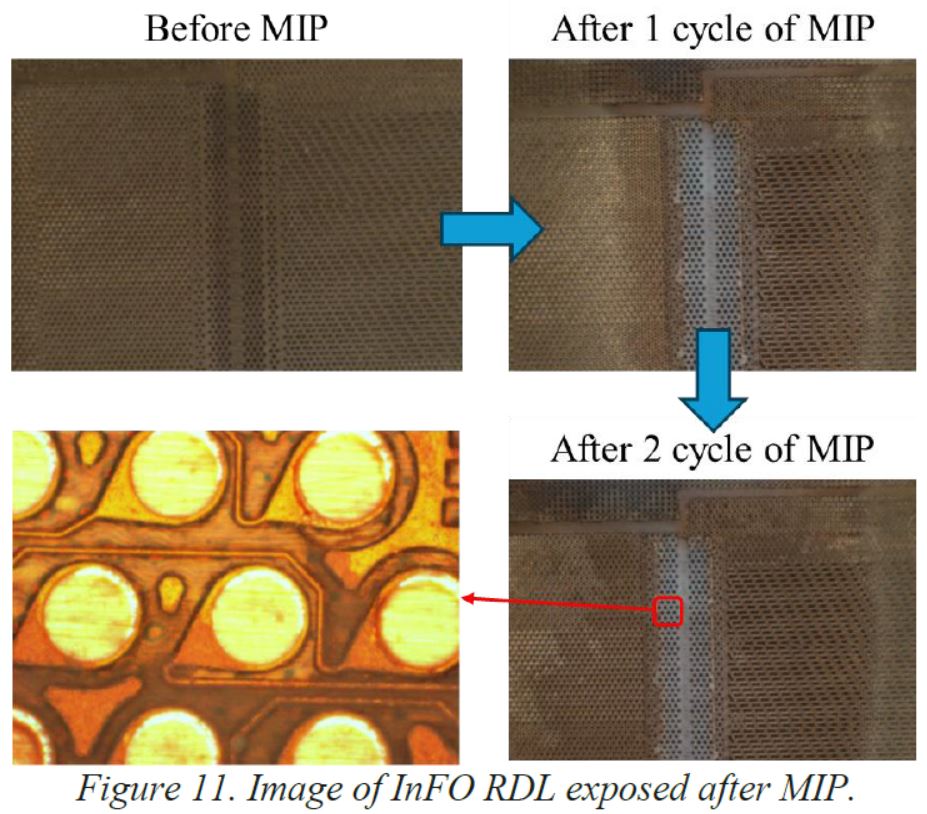
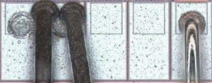
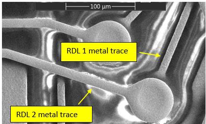
SiP has become a popular technology in recent years due to its small form factor enabled by multidie stacking. In some SiP architectures, FOW is an alternative to interposer dies, in which the wires of the lower die become embedded in the polymer film.
To expose the lower die for subsequent failure analysis, the top die can be removed with milling/polishing. Removing the remaining FOW material using acid can cause corrosion on the Cu wires of the lower die, in severe cases causing wire breakage. Corrosion and wire breakage can impact the electrical functionality, obscure original failure sites, and cause delays in subsequent failure analysis. MIP decapsulation successfully removes the FOW material, exposing the lower die, and does not damage the Cu wires.
These two case studies demonstrate how MIP decapsulation can be leveraged in failure analysis workflows, where laser and acid etching fall short. By preserving plating materials, wire integrity, and electrical functionality, MIP decapsulation enables reliable sample preparation for failure analysis on increasingly complex packages.
Interested in learning more about these two failure analysis case studies? Download:
Revolutionizing IC Package Decapsulation with Microwave-Induced-Plasma (MIP) System
Infineon, IPFA 2025, Cu Bond Wire, Repackaging.
Need more information?
Ready to include MIP as a sample preparation method in your failure analysis workflows?